| Issue |
Manufacturing Rev.
Volume 3, 2016
|
|
|---|---|---|
| Article Number | 5 | |
| Number of page(s) | 6 | |
| DOI | https://doi.org/10.1051/mfreview/2016004 | |
| Published online | 15 March 2016 | |
Research Article
Low temperature high density plasma nitriding of stainless steel molds for stamping of oxide glasses
1
Department of Engineering and Design, Shibaura Institute of Technology, 3-9-14 Shibaura, Minato-City, Tokyo
108-8548, Japan
2
Research Center, Kimura Precision, Co. Ltd., Kyoto
615-8245, Japan
3
Nano-Coat Laboratory, LLC., Tokyo
144-0045, Japan
* e-mail: This email address is being protected from spambots. You need JavaScript enabled to view it.
Received:
30
September
2015
Accepted:
25
January
2016
Abstract
Various kinds of stainless steels have been widely utilized as a die for mold- and direct-stamping processes of optical oxide glasses. Since they suffered from high temperature transients and thermal cycles in practice, they must be surface-treated by dry and wet coatings, or, by plasma nitriding. Martensitic stainless steel mold was first wet plated by the nickel phosphate (NiP), which was unstable at the high temperature stamping condition; and, was easy to crystalize or to fracture by itself. This issue of nuisance significantly lowered the productivity in fabrication of optical oxide-glass elements. In the present paper, the stainless steel mold was surface-treated by the low-temperature plasma nitriding. The nitrided layer by this surface modification had higher nitrogen solute content than 4 mass%; the maximum solid-solubility of nitrogen is usually 0.1 mass% in the equilibrium phase diagram. Owing to this solid-solution with high nitrogen concentration, the nitrided layer had high hardness over 1400 HV within its thickness of 50 μm without any formation of nitrides after plasma nitriding at 693 K for 14.4 ks. This plasma-nitrided mold was utilized for mold-stamping of two colored oxide glass plates at 833 K; these plates were successfully deformed and joined into a single glass plate by this stamping without adhesion or galling of oxide glasses onto the nitrided mold surface.
Key words: Plasma nitriding / High nitrogen solute concentration / Martensitic stainless steel / Solid solution hardening / Mold / Mold-stamping
© T. Aizawa et al., Published by EDP Sciences, 2016
 This is an Open Access article distributed under the terms of the Creative Commons Attribution License (http://creativecommons.org/licenses/by/4.0), which permits unrestricted use, distribution, and reproduction in any medium, provided the original work is properly cited.
1. Introduction
Various kinds of stainless steels have been widely utilized as a mold-die for injection molding of plastics and for mold- and direct-stamping processes of optical oxide glasses. For examples, the case-hardened AISI420 martensitic stainless steels, graded by STAVAX in commercial, is used as a mold for injection molding [1]. AISI316L austenitic stainless steels are also employed as a mold-die for direct stamping of oxide glasses [2]. In the former, heat treatment or case-hardening processes can afford to provide the sufficient hardness to molds, working around 500 K. In the latter, since the glass-transition temperature (Tg) of oxide glasses is much higher than plastics, most of molds must be coated or plasma nitrided to build up the hardened layer with heat resistance and endurance against galling [3].
In addition, these stainless steel mold substrates are often wet-plated by the nickel phosphate (NiP) [4]. Then, fine micro-textures are machined into this amorphous NiP layer; this original micro-patterns are duplicated onto the oxide glasses by mold-stamping as an optical element. However, this NiP is unstable at the high temperature stamping condition; it is easy to crystalize or to fracture by itself. This issue of nuisance significantly lowers the productivity in fabrication of optical elements at present [5].
The authors [6–8] have developed the high density plasma nitriding process for hardening of Fe-Cr binary alloys and stainless steel molds. In particular, low temperature RF-DC plasma nitriding is effective to make solid solution hardening of martensitic and austenitic stainless steels [8, 9].
In the present paper, the stainless steel mold is surface-treated by the low-temperature plasma nitriding at 693 K for 7.2 ks and 14.4 ks, respectively. First, SEM-EDX analysis is made to describe the micro-structure change; the nitrided layer by this surface modification has higher nitrogen solute content than 4 mass%. Compared to the maximum solid-solubility of nitrogen of 0.1 mass% in the equilibrium phase diagram, this high nitrogen distribution characterizes the present nitrided stainless steels. In second, XRD and XPS analyses reveal that no nitrides are synthesized as precipitates by the present plasma nitriding and that nitrogen interstitials occupy the vacancy sites in the α′-supercells. Since this occupation process accompanies with straining in crystals, the nitrided layer is hardened by this solid solution. In fact, the micro-Vickers testing proves that the nitrided layer has high hardness over 1400 HV within its thickness of 50 μm. This nitrogen solid-solution treated stainless steel has thermal resistivity even at the mold-stamping conditions up to 900 K. Two colored oxide glass plates are deformed and joined with success into an optical element by mold-stamping.
2. Experimental procedure
2.1. Plasma nitriding system
In this nitriding system, the input-and-out power matching takes place automatically around 2 MHz with the prompt duration of 1 ms at most. This high controllability enables to make full use of meso-plasma pressure range over 50 Pa. Figure 1 illustrates the present system. In this chamber, both RF- and DC-plasmas are independently ignited and controlled in the meso-pressure range. Since both the nitrogen atoms and NH-radicals work as a main activated species, the stainless steels can be nitrided even below 700 K. Heating unit is located under this DC-biased cathode plate. In the following nitriding experiments, the specimens are located on the cathode table and nitrided under the nitrogen and hydrogen mixed gas condition after pre-sputtering for 1.8 ks at 693 K. The flow-rate ratio of this mixed gas has influence on the yield of NH-radicals; after preliminary experiments [7, 8]. N2 gas flow is controlled by 100 mL/min, and, H2, by 20 mL/min, respectively. RF-voltage, DC-bias and pressure are constant by 250 V, −300 V and 70 Pa, respectively. After nitriding at 693 K for 7.2 ks or 14.4 ks, the nitrided specimens and molds are picked up after cooling down to 473 K.
 |
Figure 1. RF-DC plasma nitriding system, working even in the low temperature. |
2.2. Mold-stamping system
Mold-stamping test was performed by the CNC table-top stamping system, as shown in Figure 2. Both the applied load and stroke are numerically controlled up to 50 kN and 100 mm, respectively. Since each step in the stamping advances by 0.1 μm, fine micro-patterns can be imprinted onto the work materials by using a precise mother tool [10]. The ultrahigh frequency induction heating device, working around 2 MHz, is utilized to make rapid heating and quenching. The upper and lower molds are directly heated to sustain the holding temperature during mold-stamping. The sequential control of input power enables to suppress the temperature deviation within the tolerance of 1 K. This accurate thermal control results in high qualification in mold-stamping just above the glass transition temperature. To be free from severe oxidation, the vacuum cassette mold system is constructed so that the mold-stamping takes place under 100 Pa.
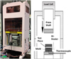 |
Figure 2. A mold stamping system for bet-shaping and joining of oxide glasses. |
2.3. Specimen and mold
Martensitic stainless steel AISI420 specimens and mold-substrates were prepared to have either surface polished. The specimen was shaped by 25 × 25 × 5 mm3; the mold substrate, the circular disc with the diameter of 25 mm and the thickness of 5 mm.
2.4. Observation and measurement
Scanning Electron Microscope (SEM) as well as Electron Diffraction X-ray (EDX) were utilized to make micro-structure analysis and to make nitrogen element mapping on the cross-section of nitrided specimens. Micro-Vickers hardness testing was performed to describe the surface hardness distribution as well as the hardness depth profile. The applied load was constant by 0.25 N (or 25 g). XPS (X-ray photoelectric spectroscopy) was also used to investigate the intrinsic chemical shift to occupation of nitrogen solutes at the vacancy site in the α′-supercells. In this measurement, the monochromic Al-Kα by 25 W was utilized with the probe diameter of 100 μm. The scanning width of energy was 0.1 eV.
3. Experimental results and discussion
3.1. Inner nitriding process
The nitrided AISI420 specimen at 693 K for 14.4 ks was halved by wire-cutting to investigate the microstructure and nitrogen solute map on its cross-section. SEM and EDX were utilized to describe the nitrogen concentration in the depth of nitrided layer. Figure 3a depicts the SEM image and the nitrogen mapping by EDX in the cross-section of nitrided martensitic stainless steel specimen, respectively. Only after nitriding for 14.4 ks, the nitrided layer thickness reaches to 50 μm.
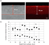 |
Figure 3. (a) SEM image and nitrogen mapping by EDX on the cross-section of nitrided layer. (b) Distributions of chromium and nitrogen solute in the depth from the surface of nitrided at 693 K for 14.4 ks. |
EDX was also utilized to measure the chromium and diffusing nitrogen contents from the surface to the depth in each step by 5 μm. Figure 3b depicts the depth profiles of both element contents. At the vicinity of surface, the nitrogen solute content becomes 9 mass% in average. The maximum solid solubility of nitrogen into irons was only 0.1 mass% after the phase diagram of Fe-N system [11]. The highest surface nitrogen contents of plasma nitrided tool steels and stainless steels by using the commercial process at 823 K was reported to be 0.1 to 0.2 mass% [12]. This high surface nitrogen content significantly characterizes the present inner nitriding process at low temperature.
The nitrogen content decreases from this high concentration at the surface down to 4 mass% in the middle range of thickness and goes to nearly zero near the nitriding front end. In particular, the plateau with constant nitrogen content around 4 mass% is formed in the range of 10–40 μm in depth. As reported in [12, 13], since every inner nitriding process in the high temperature plasma nitriding is governed by the nitrogen diffusion mechanism, the nitrogen content exponentially decreases from the surface to the depth toward the nitriding front end. This nitrogen content depth profile in the nitrided stainless steels is intrinsic to the present low temperature plasma nitriding.
On the other hand, little change is detected in the chromium concentration along the depth of nitrided layer. In fact, the average of chromium content is 12 mass%, which is the same as the initial content of AISI420 stainless steels, with the deviation of 1.5 mass%, as shown in Figure 3b. This implies that no chromium is used for precipitation reaction of CrN during plasma nitriding in different from the high temperature plasma nitriding, where large amount of chromium constituents in the matrix was used to synthesize CrN [12, 13]. Hence, the thermal and corrosion resistance, intrinsic to original stainless steels, must be never lost even after the present plasma nitriding.
XRD analysis was also performed to investigate whether the nitride precipitates were synthesized by plasma nitriding at 693 K for 7.2 ks and 14.4 ks. As shown in Figure 4, no significant peaks for nitrides were seen in the range of 30° < 2θ < 40°; e.g., little significant peaks other than a main peak at 2θ = 44° were seen in the nitrided specimen for 14.4 ks. The detected small peak detected at 2θ = 38° in the nitrided specimen for 7.2 ks might be a transient phase by solid solution process with high nitrogen content at the surface [14, 15].
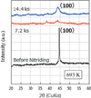 |
Figure 4. XRD diagram of nitrided AISI420 martensitic stainless steels at 693 K for 7.2 ks and 14.4 ks. |
Comparing the main peaks for (1 0 0)-plane of α′-Fe lattice before and after nitriding, the original peak at 2θ = 44.7° for AISI420 stainless steels is shifted in the lower 2θ side down to 2θ = 44°. This implies that the α′-Fe lattice structure expands itself by site occupation of nitrogen solute into vacancy sites. Hence, the presence of nitrogen solutes in the α′-supercell with 4–9 mass% in the nitrided layer accompanies with straining or distortion of original α′-lattice [16].
3.2. Solid-solution process
When the nitrogen interstitial atoms are present as a solute in the α′-supercell, its binding energy is different from the original nitrogen atom in solids with weak bonding and from the bound nitrogen in CrN. XPS is employed to analyze the binding energy of nitrogen in the nitrided layer at 693 K for 14.4 ks. First, the argon sputtering was used to clean the surface by the rate of 3 nm/min. Then, the measured energy was standardized by the carbon energy of 284.8 eV. Figure 5 depicts the XPS diagram of N1s on the surface of nitrided layer, at its center and below the nitrided layer, respectively. Fine energy profiles are detected both on the surface and in the nitrided layer. No peaks are detected below the nitrided layer.
 |
Figure 5. XPS spectra measured at the surface of the nitrided layer, at its center and below the nitrided layer. |
The measured N1s spectra have the peak at 399.6 eV. After [17], the bound N1s in CrN has the binding energy of 396.2 eV; the unbound N1s or much weakly bound N1s in the polyimide, 400.2 eV after [18]. This reveals that the nitrogen atoms present in the nitrided layer are not bound in CrN but relatively weak-bound in the α′-supercell. Further precise XPS analysis and discussion is needed to define the binding state of nitrogen solutes in the nitrided layer.
The above EDX and XPS analyses suggest that the nitrogen solute is structured into α′-supercell through its occupation of vacancies and have weaker bonding than nitrogen in CrN. After the first principle calculation on the occupation of nitrogen atoms in the α′-supercell in [19], let us consider this occupation process during the present plasma nitriding. From the nitrogen mapping by EDX, N/(N + Fe) ratio is 27 to 28 at.%, corresponding to 9 mass%, at the vicinity of surface and that N/(N + Fe) ratio is 15–17 at.%, corresponding to 4 mass%, in the middle of the nitrided layer except for the vicinity of nitriding front end. Assuming this occupation process is driven by nitrogen concentration from the surface, both the octahedral and tetrahedral vacancies, or, Voct and Vtra are expected to be gradually occupied by nitrogen interstitials from the surface. At the vicinity of surface with higher nitrogen content around 9 mass%, two pairs of Voct and Vtra are occupied by nitrogen solutes. One pair of Voct and Vtra are occupied to invoke two nitrogen solutes into the α′-supercell in the middle of the nitrided layer.
3.3. Solid solution hardening
ASIS420 specimen with two stripe masks on its surface was prepared and nitrided at 693 K for 7.2 ks to investigate the hardness distribution across these two stripe masks along the center-line on the specimen surface as shown in Figure 6a. Since the masked regions are free from nitriding and remain as they were before nitriding, the measured hardness is equivalent to the AISI420 matrix hardness of 250 HV. On the other hand, the unmasked or nitrided regions have much higher hardness than 1400 HV even after plasma nitriding for 7.2 ks.
 |
Figure 6. (a) Variation of the surface hardness distribution measured across two masking stripes on the nitrided specimen at 693 K for 7.2 ks. (b) Hardness depth profiles of the nitrided region in the two-stripe masked specimens at 693 K for 7.2 ks and 14.4 ks, respectively. |
Figure 6b depicts the hardness depth profile of nitrided region in the two-stripe masked specimen at 693 K for 7.2 ks and 14.4 ks, respectively. As seen in Figure 6a, high surface hardness is attained to be 1600 HV for 7.2 ks and 1800 HV for 14.4 ks, respectively. This high hardness monotonically decreases in the depth of nitrided layer toward the nitriding front end. Comparing this hardness depth profile for 14.4 ks to the nitrogen content depth profile in Figure 3b, high nitrogen concentration from the surface to the depth of 50 μm corresponds to high hardness layer in the nitrided region in depth. This proves that solid solution with high nitrogen contents drives the hardening process of stainless steels.
3.4. Hot mold-stamping test
The nitrogen solid-solution hardened AISI420 stainless steel has dense microstructure with nitrogen solute occupation into α′-supercell. Its surface property as well its engineering endurance are improved from the martensitic stainless steels before nitriding. In order to demonstrate this possibility, the nitrided AISI420 substrate at 693 K for 14.4 ks was shaped to fabricate a flat mold for hot mold-stamping of oxide glasses.
In this experiment, two colored oxide glass plates with different glass transition temperature (Tg) and thickness were mold-stamped at 833 K for 3.6 ks in vacuum atmosphere under 100 Pa by using this nitride mold. Using the programmed thermal cycling schedule, the stamped glasses are free from fracture. Figure 7a depicted the cross-section of two oxide glass plates and nitrided mold. Under the reduction of thickness by 8%, two oxide glasses were uniformly compressed and joined together with each other. Figure 7b shows the jointed glass plate after demolding from the nitrided mold. A joined two-color glass product is successfully fabricated to have no defects and cracks.
 |
Figure 7. Hot mold stamping to join two colored oxide glass plates to one optical element at 833 K. (a) Two color oxide glass sheets on the molds. (b) Deformed and joined two-color oxide sheet. |
This success in hot mold-stamping implies that the α′-supercell structure occupied by nitrogen solutes at the vacancy sites could promote the heat resistance of original AISI420 stainless steels in vacuum. Further research is needed to prove the improvement of thermal endurance of this plasma nitrided molds by the hot hardness testing.
4. Conclusion
The solid-solution hardened stainless steels by low temperature plasma nitriding work as a heat resistant mold for hot stamping and injection molding of oxide glasses and high-Tg plastics. This mold with the nitrided layer thickness over 50 μm and the surface hardness over 1400 HV by nitriding at 693 K for 14.4 ks or 4 h, is attractive for mold-stamping of optical elements since it is free from hot galling and severe abrasive wear. In particular, the average nitrogen solute content of 4 mass% or 15 at.% is useful to prevent the hot-stamping mold from galling with oxide glasses in the hot and vacuum conditions. Further studies are planned to utilize this nitrided AISI420 material for shaping and machining to have well-defined geometry to optical element and to use it as a mold to duplicate its geometry into the high-Tg oxide glasses with sufficient accuracy in dimension.
5. Implications and influences
The present paper has contribution to surface treatment for dies and molds. In particular, low temperature plasma nitriding is used to make solid solution hardening of stainless steel mold. This mold is utilized for mold-stamping of oxide glasses. Two colored oxide glass sheets are uniformly deformed and joined into a single optical glass.
Acknowledgments
The authors would like to express their gratitude to Mr. S. Kurozumi and Mr. H. Yamagata (Shibaura Institute of Technology) for their help in mold stamping experiments of oxide glasses. This study is financially supported by MEXT with the contract of # 411419.
References
- T. Aizawa, F.-J. Hoe, S. Yukawa, Res. Rep. SIT 55 (2011) 34–43. [Google Scholar]
- A. Ikeda, T. Fukuda, MITI-supporting industry report on the surface treatment of molds for oxide glass stamtry, 2013-SIR-05 (2013) 113–116. [Google Scholar]
- K. Dohda, T. Aizawa, Manuf. Lett. 2 (2014) 82–85. [CrossRef] [Google Scholar]
- http://www/nacro.co.jp (cited in 12/24/2015) [Google Scholar]
- K. Okada, Y. Hirata, K. Nitta, S. Inazawa, SEI-Technical Review 167 (2005) 92–95. [Google Scholar]
- T. Aizawa, Y. Sugita, Prof. 6th SEATUC Conference, Bangkok, 2012. [Google Scholar]
- T. Aizawa, T. Fukuda, K. Itoh, Int. Steel Res. 87 (2012) 215–220. [Google Scholar]
- T. Aizawa, Y. Sugita, Res. Rep. SIT 57 (2013) 1–10. [Google Scholar]
- M. Anzai (Ed.), Surface treatment for high qualification of dies and molds, Nikkan Kogyo Shimbun, Japan, 2009, pp. 43–61. [Google Scholar]
- T. Aizawa, K. Itoh, T. Inohara, Proc. 6th ICOMM (2010) 77–82. [Google Scholar]
- Japan Institute of Metals (Ed.), Metals Data Book (Maruzen, Tokyo, 1974), p. 25. [Google Scholar]
- Y. Hiroka, K. Inoue, Denki-Seiko 80 (2010) 15–24. [Google Scholar]
- N. Granito, H. Kuwahara, T. Aizawa, J. Mater. Sci. 37 (2002) 835–844. [CrossRef] [Google Scholar]
- D. Santojojo, T. Aizawa, M. Shinji, H. Morita, Proc. 8th ICOMM 90 (2014) 1–8. [Google Scholar]
- Abdelrahman, T. Aizawa, Proc. 10th SEATUC, Tokyo (2016) (CD-ROM). [Google Scholar]
- D. Manova, et al., Nucl. Instrum. Methods Phys. Res. B 242 (2006) 285–288. [CrossRef] [Google Scholar]
- F. Esaka, et al., Surf. Sci. 16 (1997) 42–47. [Google Scholar]
- G.M. Rignasese, et al., Phys. Rev. Lett. 79 (1997) 5174–5180. [CrossRef] [Google Scholar]
- C. Domain, et al., Phys. Rev. B 69 (2004) 114112. [CrossRef] [Google Scholar]
Cite this article as: Aizawa T, Fukuda T & Morita H: Low temperature high density plasma nitriding of stainless steel molds for stamping of oxide glasses. Manufacturing Rev. 2016, 3, 5.
All Figures
|
Figure 1. RF-DC plasma nitriding system, working even in the low temperature. |
| In the text | |
|
Figure 2. A mold stamping system for bet-shaping and joining of oxide glasses. |
| In the text | |
|
Figure 3. (a) SEM image and nitrogen mapping by EDX on the cross-section of nitrided layer. (b) Distributions of chromium and nitrogen solute in the depth from the surface of nitrided at 693 K for 14.4 ks. |
| In the text | |
|
Figure 4. XRD diagram of nitrided AISI420 martensitic stainless steels at 693 K for 7.2 ks and 14.4 ks. |
| In the text | |
|
Figure 5. XPS spectra measured at the surface of the nitrided layer, at its center and below the nitrided layer. |
| In the text | |
|
Figure 6. (a) Variation of the surface hardness distribution measured across two masking stripes on the nitrided specimen at 693 K for 7.2 ks. (b) Hardness depth profiles of the nitrided region in the two-stripe masked specimens at 693 K for 7.2 ks and 14.4 ks, respectively. |
| In the text | |
|
Figure 7. Hot mold stamping to join two colored oxide glass plates to one optical element at 833 K. (a) Two color oxide glass sheets on the molds. (b) Deformed and joined two-color oxide sheet. |
| In the text | |
Current usage metrics show cumulative count of Article Views (full-text article views including HTML views, PDF and ePub downloads, according to the available data) and Abstracts Views on Vision4Press platform.
Data correspond to usage on the plateform after 2015. The current usage metrics is available 48-96 hours after online publication and is updated daily on week days.
Initial download of the metrics may take a while.